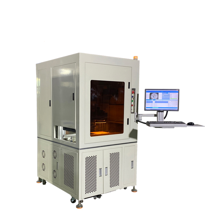
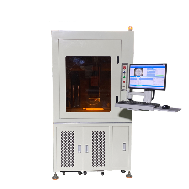
Key Features of PCB Laser Marking Machines
- Ultra-High Precision & Miniaturization
- Achieves micron-level accuracy (as fine as 0.05 mm) for marking tiny QR codes, serial numbers, or logos on small PCB surfaces (down to 3×3 mm), ideal for modern compact electronics.
- Advanced UV or fiber lasers ensure crisp, permanent marks without damaging delicate substrates like flexible circuits or thin copper layers.
- Non-Contact, Zero Mechanical Stress
- Laser marking eliminates physical contact, preventing scratches, deformation, or contamination of sensitive PCB components.
- Suitable for fragile materials (e.g., FPC flexible boards) and pre-coated surfaces.
- Broad Material Compatibility
- Effective on metals (copper, aluminum), FR-4 substrates, ceramics, and composite materials used in PCB manufacturing.
- Adapts to textured or uneven surfaces, ensuring consistent mark quality across diverse PCB types.
- Automation & Smart Integration
- Seamless integration with SMT production lines, robotic arms, and IoT-enabled systems for 24/7 unmanned operation.
- High-precision CCD cameras enable automatic positioning, real-time quality inspection, and MES system data synchronization for traceability.
- Eco-Friendly & Safe Operation
- No consumables (inks, solvents) or hazardous waste, aligning with global environmental regulations (e.g., RoHS, REACH).
- Eliminates toxic fumes and chemical exposure, ensuring operator safety.
Core Advantages of PCB Laser Marking Technology
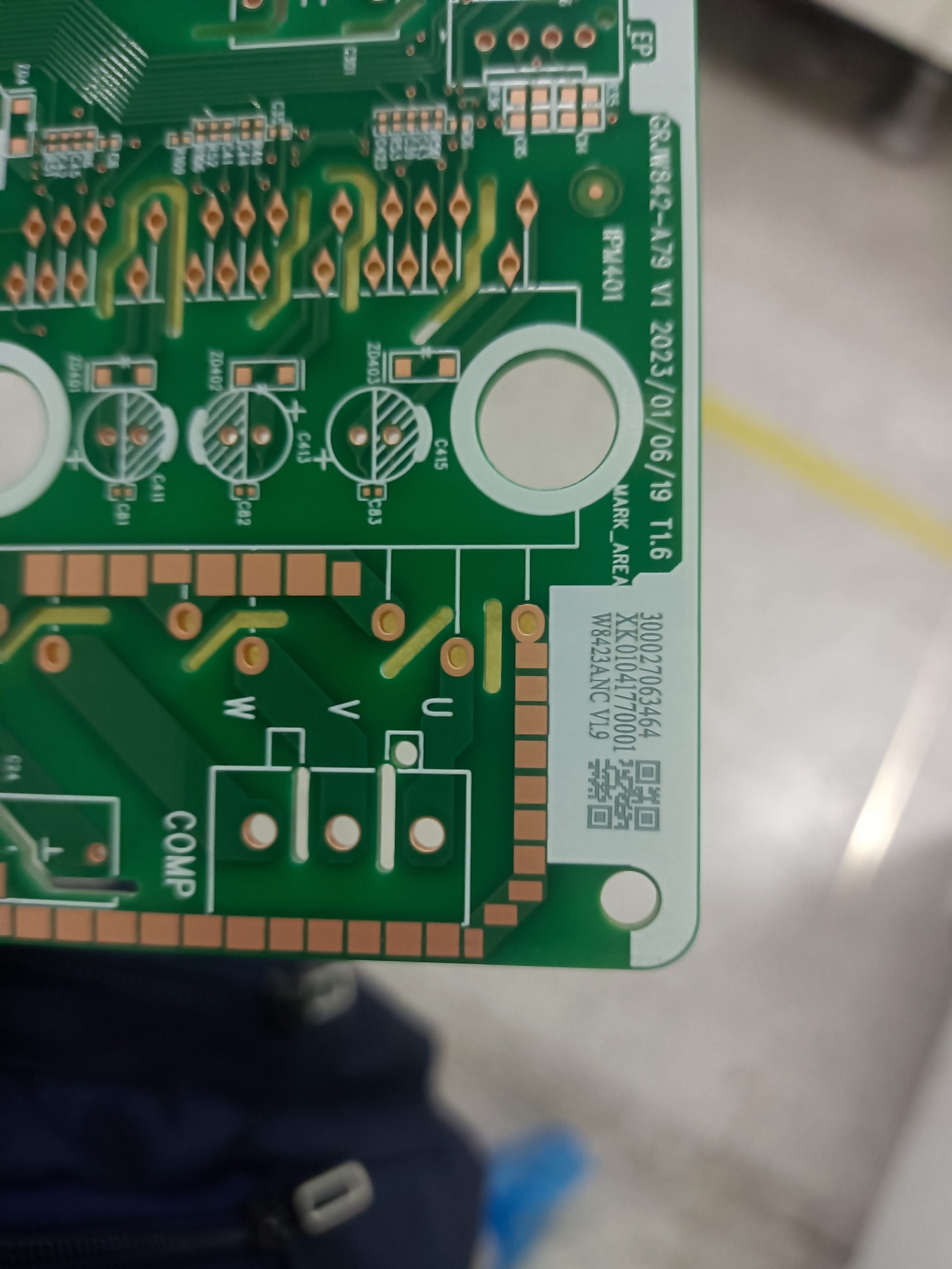
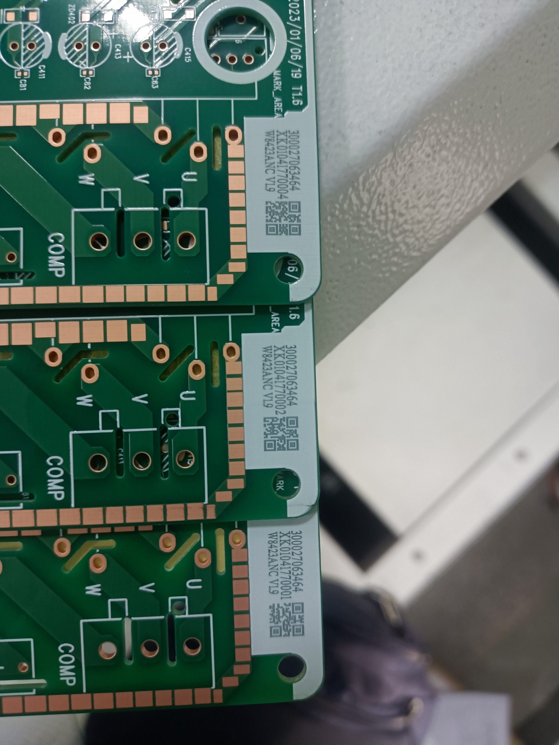
- Permanent, Tamper-Proof Markings
- Laser-etched codes resist abrasion, chemicals (e.g., cleaning agents, acids), and environmental factors (UV, humidity), ensuring lifelong traceability.
- Critical for anti-counterfeiting and compliance with FDA, EU, or automotive industry standards.
- High-Speed Production & Cost Efficiency
- Marks PCBs in 0.5–2 seconds per unit, boosting throughput by 5–10x compared to traditional silk screening.
- Low operating costs: No consumables, minimal energy consumption, and reduced scrap rates via AI nesting software.
- Superior Flexibility & Customization
- Instantly switch between designs (text, barcodes, 2D codes) via CAD/CAM software, enabling rapid prototyping and mass production.
- Supports 360° marking on cylindrical components and complex geometries with rotary axis attachments.
- Enhanced Product Quality Control
- Automated defect detection and real-time data logging ensure 100% traceability from raw materials to finished products.
- Reduces human error and improves yield rates in high-volume manufacturing.
- Future-Ready Industry 4.0 Compatibility
- Cloud-based analytics enable predictive maintenance, remote diagnostics, and digital twin simulations for optimized workflows.
- Integrates with MES/ERP systems for end-to-end production monitoring and smart factory automation.
Primary Industrial Applications
- Consumer Electronics
- Traceability marking on smartphone PCBs, wearables, and IoT devices.
- Automotive & Aerospace
- Durable coding on engine control units (ECUs), sensors, and avionics PCBs.
- Medical Devices
- Biocompatible markings on implantable device circuits and diagnostic equipment.
- Industrial IoT & Energy
- Serialization of power supply boards, solar inverters, and industrial controllers.
Why Choose Our PCB Laser Marking Solutions?
- Tailored Configurations: Systems from 3W UV lasers (for fine-pitch FPCs) to 300W fiber lasers (for high-speed metal PCBs).
- Smart Software Suite: Pre-loaded industry templates, AI-driven parameter optimization, and MES/ERP connectivity.
- Global Compliance: CE, ISO 13485 (medical), and IATF 16949 (automotive) certifications.
- Lifetime Support: 24/7 technical assistance, on-site training, and global spare parts logistics.
Reviews
There are no reviews yet.